Phase A. Design schematic and Layout
After installing Eagle, add the necessary components libraries to it. To accomplish this:
- download following libraries: eagle_fab.lbr , ATTINY412-SSF.lbr and SparkFun-Connectors.lbr
- and put those in the "library" folder of your Eagle. (or you can put those anywhere in your computer and define from Options > Directories (Fig. 1) where Eagle should look for those).
- To activate libraries, select each library from the left menu, right click on it and check the 'use' box (Fig. 2).
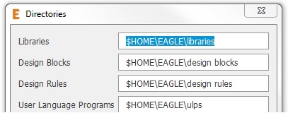
Figure 1. You can define library path in Eagle
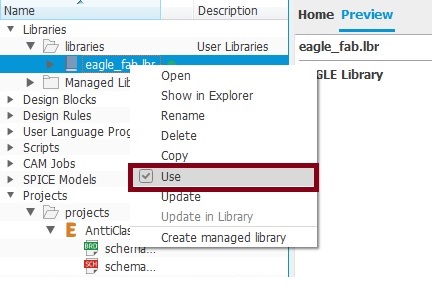
Figure 2. Here you can activate fab lab library
For this week, our task was to re-design an existing board
(echo board designed by Neil), and add a button and a LED to it. I did choose ATtiny412 based board, because it seems to be quite common in ealier years' assignment description. In practise, it means, that I can follow tutorials and crosscheck my own design to earlier ones.
Here is a summary of the steps that you can follow to draw the schematic and layout:
Design Schematic
- Create a new project in Eagle from File > New > Project.
- To Create a new Schematic (.sch), right click on your project in the left menu, then New > Schematic
- Add the components you need from eagle_fab library, with Add Part tool (See Figure. 3).
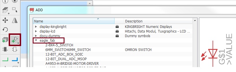
Figure 3. How to add components?
- To add a value to each component, right click on it and select Value.
- Add GND and VCC from supply1 library with the Add Part tool.
- Wire the components with the Net tool.
- Check the correctness of the schematic by Electric Rule Check (ERC) (from the left menu).
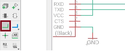
Figure 4. Wire components by using Net-tool
Figure 5 shows the final view of this schematic.
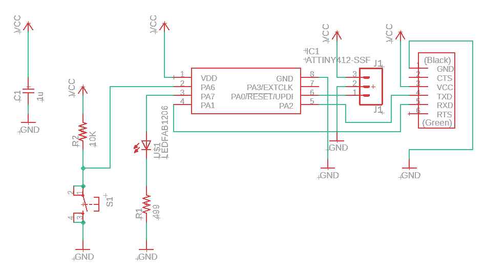
Schematics of my board
Layout
- Go to board editor by clicking on Generate/Switch to board icon (see Figure. 6).
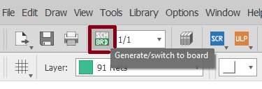
Figure 6. How to switch into board editor
- Click on Move icon in the left menu to move the components to their place, so that you can minimize the wire length.
- Define the Design Rules Check (DRC) parameters (e.g. minimum clearance) from Tools > DRC... (See Figure. 7). The minimum clearance cannot be less that the diameter of the milling bit that you plan to use.
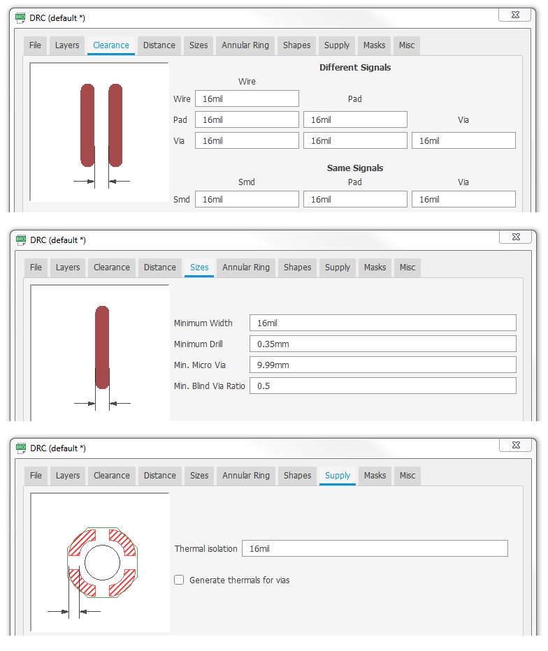 Figure 7. Defining Design Rules Check (DRC) parameters.
- Click "Autorouter" button on the left menu to explore possible routes of components (see figures 8 and 9 below).
- Remember to set Bottom N/A to make the one side board.
- Select the highest possibility option
- When you get 100% possibility of routing, check the board layout by doing DRC test (Tools > DRC) to be sure that there are not erros
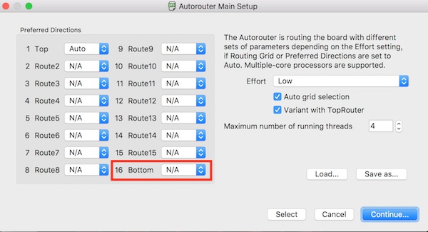
Figure 8. Autorouter settings
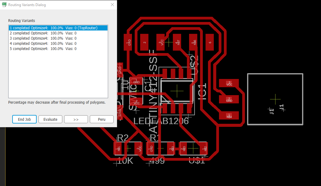
Figure 9. Results from the autorouting.
- When the routes between the components are ready, modify the size of the board. The board area is defined by the dimension layer (layer 20). Simply drag it to change it to your desired size.
- To make the ground fills, follow these steps:
- In the top menu bar, make sure the top layer is selected.
- Click on the polygon icon in the left menu.
- Route the polygon in the shape you want it. Make sure to close it at the starting point. A polygon with a dashed line will appear.
- To connect the polygon to ground, right click on the dash line and select Name. Name the polygon GND (Fig. 9).
- Click on Ratsnest icon in the left menu.
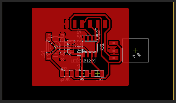
Figure 10. Connect the polygon to the ground.
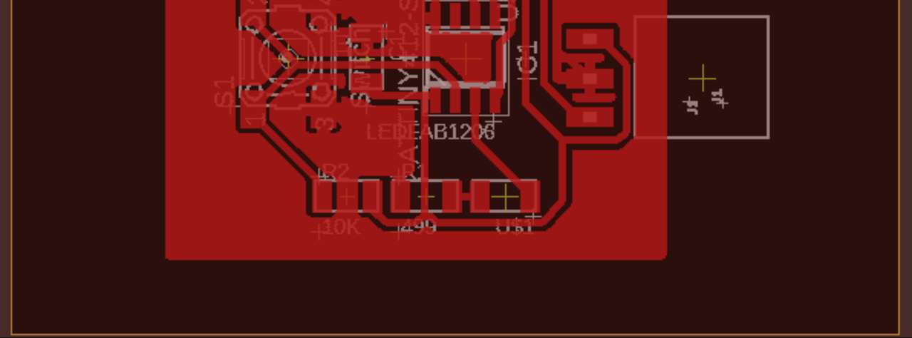
- To draw the outlines for cutting, set the working layer to Milling (layer 46), and draw the the outline with Line tool from the left menu. Outlines must be thicker than the diameter of the milling tool that you are going to use for cutting the outlines. Since I was going to use a 1mm milling bit, I set the outlines width to 40mil (=1.016mm). Figure 10 shows the final view of my PCB layout.
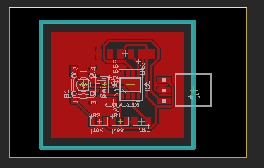
Figure 11. PCB layout of my board.
- Last step is to prepare design to be exported as an image:
- options > set > Misc > unchecking the following:
- Display and Names
- Display signal names on pads
- Display signal names on traces
- Next export image of traces:
- Layer setting > hide layers and select only top view
- File > export > Image:
- resolution:1500 dpi
- Monochrome
Phase B. Mill the PCB Board
After exporting .png-files (traces and outline for board) you have necessary items to continue to milling. Milling prodecures are exactly same than it was in the assignment: electtronics production, so I won't describe steps in the details here. Instead, I will add figures which show mods-configuration and end result of using MODS (view into .rml -files)
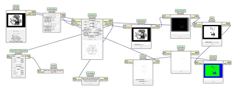
Figure 12. View on MODS interface, while I was generating traces .rml-file
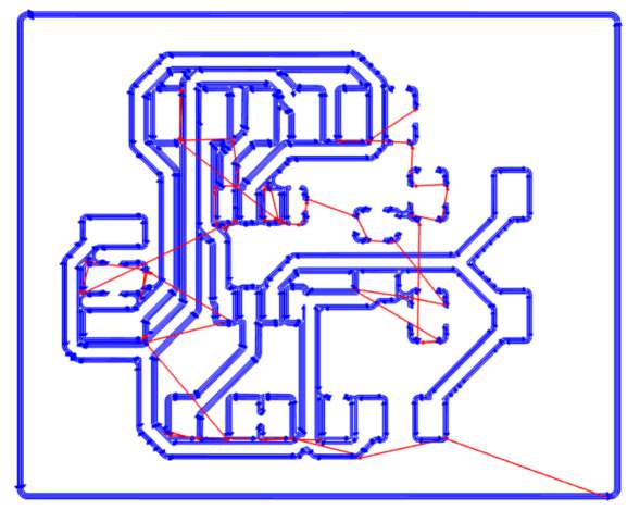
Figure 13. Result: Calcutlated routes that Roland milling machine will mill to PCB when doing traces
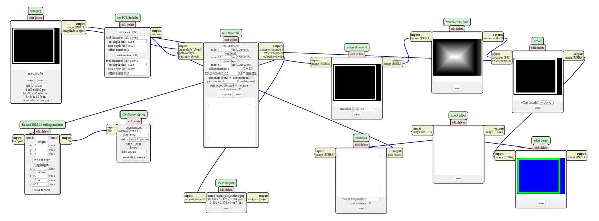
Figure 14. View on MODS interface,when I was creating outline .rml-file

Figure 15. Outlines after calculation
Phase C. Solder the components to the PCB board
Get list of components from Eagle
Before soldering, you need to gather components. I recommend you to open schematics file in Eagle, and then use "file / export / partlist" to get list of components required. Partlist is actually done based on your schematics design!
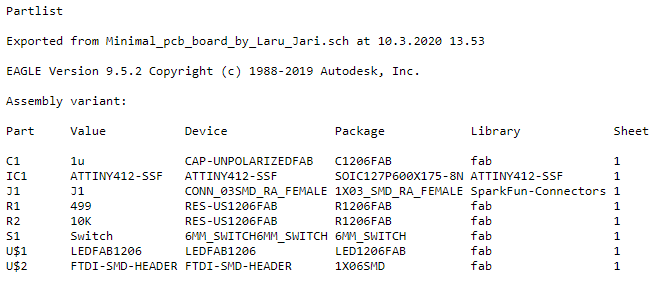
Figure 16. Partlist
Soldering the components
I won't describe soldering phase in the details, because that documentation is already done in the electronic production -task.. However, figure below shows my setup when I was soldering this circuit board, there is major difference when compared to earlier one in electronics production
I didn't found scaffolding structure (cube with circle to turn pcb) and I had to braistorm what would be good replacement. I found that I carry on my circuit board designs in Tupperware storage box and lid of that would be actually quite nice replacement.
I found that Tupperware lid was actually pretty nice platform for soldering. I didn't needd to attach it to table, because friction was good enough just when I taped PCB on the lid and started to solder. Recommended!
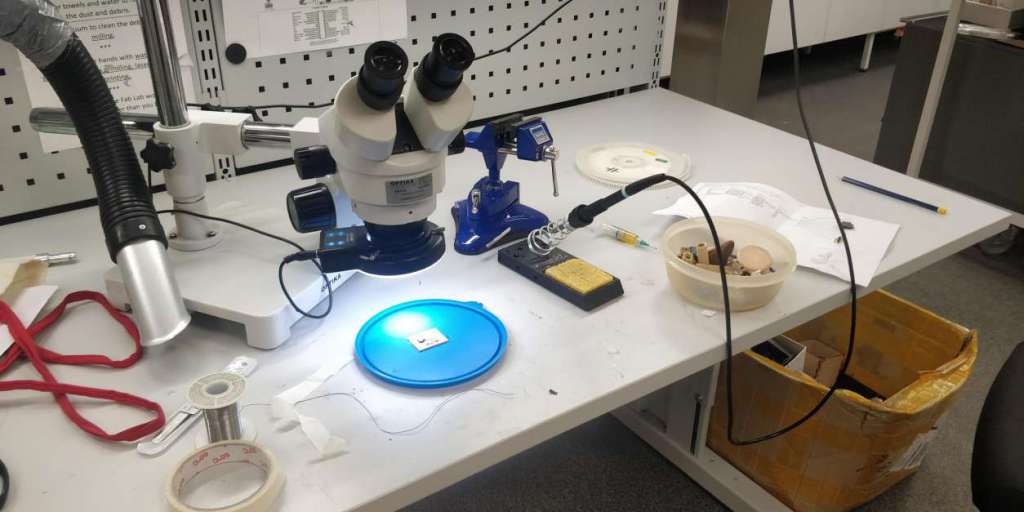
Figure 17. My soldering setup
All components soldered, board ready for testing
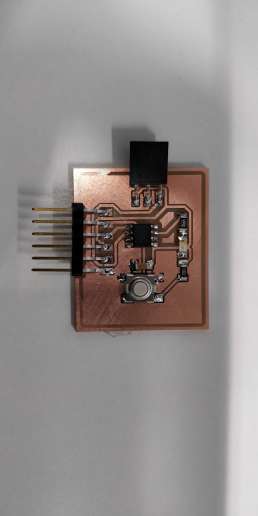
Figure 18. circuit board ready
Phase 4. Programming the board
because programmer for programming the board was task for week: electronics production, the procedures are already familiar for compiling and uploading the code to the board
For simple testing, echo-sketch is good tool
//
// hello.t412.echo.ino
//
// tiny412 echo hello-world
//    115200 baud
//
// Neil Gershenfeld 12/8/19
//
// This work may be reproduced, modified, distributed,
// performed, and displayed for any purpose, but must
// acknowledge this project. Copyright is retained and
// must be preserved. The work is provided as is; no
// warranty is provided, and users accept all liability.
//

#define max_buffer 25

static int index = 0;
static char chr;
static char buffer[max_buffer] = {0};

void setup() {
   Serial.begin(115200);
   }

void loop() {
   if (Serial.available() > 0) {
      chr = Serial.read();
      Serial.print("hello.t412.echo: Jari Laru (FabAcademy2020) typed \"");
      buffer[index++] = chr;
      if (index == (max_buffer-1))
         index = 0;
      Serial.print(buffer);
      Serial.println("\"");
      }
   }
Following procedures should be used:
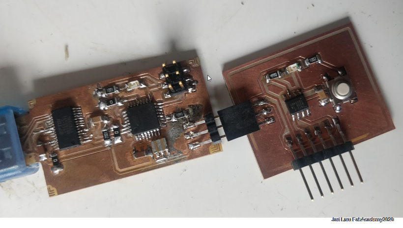
- Connect programmer to PC with USB cable and new board to programmer via JTAG connector (see the image)
- Choose board: ATtiny412/..
- Chip: ATtiny412
- Port: COM_ (check your serial prot by using device manager)
- Programmer: jtag2updi
- Press verify and upload to compile code
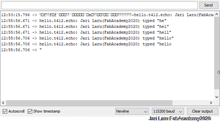
Then I opened serial monitor in Arduino IDE (with the same baudrate (115200) than specified in the code above). Code works succesfully, as you can see from the image below:
Reflections
During this week I got the idea how to solder surface mounted components. It was pretty new thing for me and it took time to learn procedures. I also learnt basics of using Eagle.
Files:
.rml)
.rml)